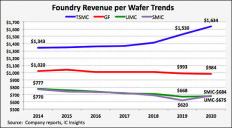
It allows to keep PV going, with more focus towards AI, but keeping be one of the few truly independent places.
-
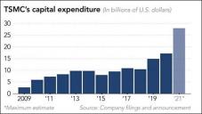
Throughout 2020, TSMC had to update its budget for expanding production and mastering new technical processes almost monthly. As a result, it reached $ 18 billion, but this year the company is going to spend a record $28 billion on specialized needs.
TSMC becoming sacred cow, hence the change of US attitude toward Taiwan.
Almost all TSMC factories are wrongly located in very risky areas.
-
Both TSMC and UMC are expected to sustain full capacity utilization for 28nm manufacturing process at their 8-inch and 12-inch fabs throughout third-quarter 2021, with gross margins from the mature node hitting new records.
It means that they are rising prices and they need to to finance 2nm and 3nm projects where they try to stop for another 8-10 years.
-
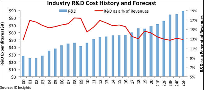
Research and development spending by semiconductor companies worldwide is forecast to grow 4% in 2021 to $71.4 billion after rising 5% in 2020 to a record high of $68.4 billion, according to IC Insights’ new 2021 edition of The McClean Report—A Complete Analysis and Forecast of the Integrated Circuit Industry. Total R&D spending by semiconductor companies is expected to rise by a compound annual growth rate (CAGR) of 5.8% between 2021 and 2025 to $89.3 billion.
Total semiconductor R&D spending has declined in only four years since the end of the 1970s (-1% in 2019 during an economic slowdown, -10% in 2009 after the industry was hit by a major global recession, and back-to-back drops of -1% in 2002 and -10% in 2001 when an economic downturn coincided with the implosion of the Internet “dot-com” bubble at the turn of the century). In the aftermath of the global recession of 2008-2009, R&D spending recovered strongly in 2010 and 2011, but then outlays slowed during the rest of the last decade for a variety of reasons, including ongoing uncertainty about the global economy and an historic wave of acquisitions in the chip industry.
Since the year 2000, total semiconductor R&D spending as a percent of worldwide sales has exceeded the four-decade historical average of 14.6% in all but five years (2000, 2010, 2017, 2018, and 2020).
Intel continued to top all other semiconductor suppliers in R&D expenditures in 2020, accounting for about 19% of the industry’s total. However, cost cuts, the elimination some product categories, and a drive to maximize efficiencies resulted in a 4% decrease in Intel’s R&D outlays in 2020 to an estimated $12.9 billion after its spending declined 1% in 2019, when its share was 22% of the industry’s total. The 2019-2020 drops in Intel R&D expenditures were the first consecutive annual declines for the company since 2008 and 2009. The 4% decrease in 2020 was the largest R&D decline for Intel since the mid 1990s. Second-ranked Samsung increased its R&D spending by 19% in 2020 to $5.6 billion partly because the South Korean memory giant stepped up development of leading-edge logic processes (of 5nm and below) to compete in the advanced IC foundry business with market leader Taiwan Semiconductor Manufacturing Co., which raised its expenditures on research and development by 24% to nearly $3.7 billion last year.
You can see both extreme greed and monopolization from this.
The wall is very near and now all companies are unprepared, TSMC just have highest speed and it will be hit hardest in time.
 sa16260.jpg658 x 292 - 44K
 -
TSMC has already struck a deal with Intel under which the pure-play foundry will use 3nm process technology to manufacture the US vendor's core CPU products, with volume production scheduled for the second half of 2022, according to sources.
So it is only one "3nm" process now. Fake 3nm, of course, but still.
-
Nvidia and Qualcomm reportedly have already reached agreements with TSMC for capacity support from its next-generation manufacturing processes,
All eggs will be in one basket and it can fall from the cliff.
-
TechNews reports that TSMC's 3nm production quotas have been distributed until 2024. The company intends to expand the new stage of lithography in four stages. "The right of the first wedding night", as noted, will traditionally go to Apple, which will be the first to start receiving 3nm products among all TSMC customers.
The next three waves will include AMD, NVIDIA, Xilinx, Qualcomm and some others, according to Taiwanese sources.
Initially TSMC will be able to process up to 55 thousand silicon wafers with 3-nm products per month per month, and by 2023 the volumes will grow to 105 thousand silicon wafers per month. The new process technology will increase the density of transistors by 70%, as well as either increase the speed by 15% with constant power consumption, or reduce energy consumption by 30% compared to the 5nm process technology. According to preliminary estimates, TSMC is ready to invest $ 71.6 billion in the development of 3-nm technology.
It is expected that 3nm chip design and manufacturing will cost around 1.5-1.7x more compared to present 5-7nm processes. So, for around 15% performance gain during non intense tasks you also will pay around 20-30% premium. New processes now become more expensive for each unit of chip performance, progress turned into regress.
-
TSMC is believed to have been under political pressure to set up an advanced wafer fab locally in the US in the wake of the US-China trade war.
Who could have though...
-
According to reports, SMIC is planning to build a new SN1 factory in Shanghai to manufacture chips on 12 "(300 mm) wafers. On this production line, the company will be able to produce up to 35,000 wafers per month, following advanced manufacturing processes below 14 nm. It is planned to spend $ 12 billion on the enterprise. SMIC is moving forward in the development of 7-nm chip production, but now its plans are hampered by the inability to purchase equipment for printing in deep ultraviolet (EUV) range due to US sanctions. This lithography uses shorter wavelengths of light and allows for more efficient downsizing of transistors.
-
China's industry ministry said this week that it met with automotive and chip manufacturers to try and help ease what is now being called a "crisis" of a shortage in global semiconductors.
Shortage of chips in auto industry seems like bad reason to keep auto production at low levels reached during COVID. As most of them are made on old lines and always had been very predictable.
Something went off in original COVID plan so some pause formed.
-
TSMC's board approved capital appropriations of about US$11.8 billion for fab construction and installation of fab facility systems, installation and upgrade of advanced technology capacity, as well as other purposes including installation of mature and specialty technology capacity, installation and upgrade of advanced packaging capacity, and second-quarter 2021 R&D capital investments and sustaining capital expenditures.
TSMC's board also approved a NT$2.50 per share cash dividend for the fourth quarter of 2020, when the company reported net profits hit a record high of NT$142.77 billion or NT$5.51 per share.
-
Chip shortage likely to persist through 2022, says Silicon Motion: Foundry and backend capacity constraints resulting in a global shortage of semiconductors will likely persist through 2022, according to Silicon Motion Technology, a Taiwan-based NAND flash device controller specialist.
Car chips shortages showed that COVID had been already used to hide big issues in manufacturing. As car sales rebounded too fast it can be seen in full force.
-
Recently Taiwan authorities asked manufacturers to reduce the consumption of water for production. This is the second order in two months. In January, large producers were advised to reduce their water consumption by 7%, and a new order requires an additional 11% reduction in the cities of Taoyuan, Taichung, Hsinchu and Miaoli. This directly affects TSMC and other semiconductor manufacturers, but the authorities assure that everything is under control.
TSMC, UMC and other manufacturers have implemented a number of dynamic water allocation measures for the Hsinchu Technology Park. Against this background, there were even rumors that the authorities in 60 days will stop the supply of water to technological parks, but there is no official confirmation of this. However, it should be expected that if the drought gets worse, the ministry will be forced to take more drastic measures to regulate water consumption.
Taiwan is worst place for chips production, best place is in the middle of big tectonic plate (biggest costs go to ensure stability) and with lot of water, cheap electricity and other stuff. Yes, I mean Siberia, but this is not an option for capital now.
-
TSMC has issues with scaling 5nm
TSMC is slow expanding capacity for 5nm process to meet strong demand from a host of heavyweight clients, including Apple, AMD and MediaTek. The foundry house's capacity for 5nm process is expected hike only by one third in second-half 2021 compared to that in the last quarter of 2020.
5nm capacity now is mostly being distributed during talks with US government as they determinate who will get the ability to make such chips and who will get free money to get equipment.
-
According to J.P. Morgan, semiconductor supply volumes in various industries are 10-30% lower than the needs of these industries. In order for the industry to be able to increase production volumes, it takes from 6 months to a year. Accordingly, throughout this period, we will observe problems with the supply of various systems and devices where chips are used.
According to various analysts, the reason for the deficit is that under the influence of the pandemic everything and everyone is being digitalized, company employees work remotely, and the demand for equipment and, accordingly, chips is increasing. But the industry, with all its desire, is not yet able to increase production volumes.
In reality we have two things:
- Capitalist owners just get record profits and do not want to increase production as long as they can
- 5nm and up require huge direct newly printed money injections that are no impossible to hide (TSMC will get around 100 billions from US and EU, free of charge). This was TSMC and few other giants are no longer even remotely independent companies, but more like governments war machines.
-
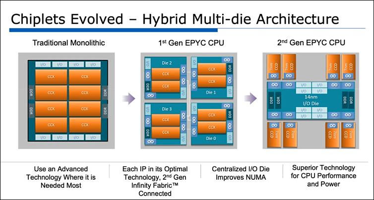
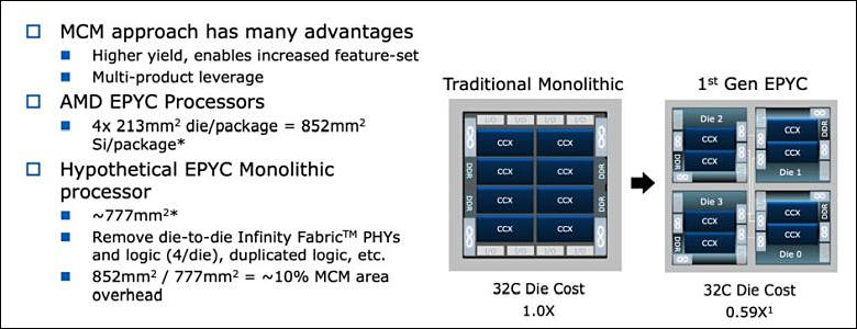
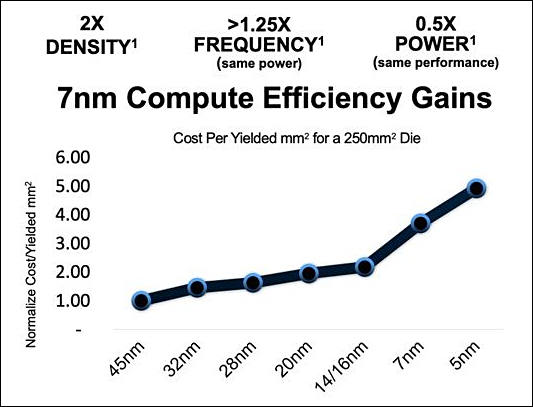
AMD Chiplets

 sa16584.jpg754 x 404 - 63K
 sa16585.jpg780 x 300 - 50K
 sa16586.jpg533 x 407 - 33K
 -
Qualcomm will continue to fabricate its next-generation 5G mobile chip, tentatively dubbed Snapdragon 895, at Samsung Electronics built using an upgraded 5nm process, but may switch to TSMC in 2022 using its 4nm process, according to industry sources.
Samsung has severe issues now with making GPUs, makes lot of silicone waste still.
TSMC also nearly full progress stop and try to keep everything almost same in 4nm version, as they can't jump to 3nm still.
-
TSMC has prioritized expanding 12-inch fabs over 8-inch ones, and it may be easier for the foundry house to squeeze in extra orders from some clients its 12-inch fabs in the second quarter, according to industry sources.
12-inch based production has lot of issues, including much more defects in source material.
TSMC hope that lot of small chiplets and such 4-5nm things will allow it to still be more profitable.
-
More issues
The shortage of semiconductor chips is gradually increasing in the world. Experts estimate the volume of the deficit at 10-30%. Any additional negative factor can increase the shortage of components, which, of course, affects all other industries - the production of laptops, desktops, servers, even cars. And such factor exists now -Samsung Corporation has not yet resumed semiconductor production at its US factory in Texas.
The problem started in mid-February - then in Texas there was an unprecedented cold, which required increased energy consumption. The South Korean company was forced to stop the work of two factories in Austin at once. The decision was unprecedented. In addition to Samsung, NXP Semiconductors, Infineon Semiconductors, and others were forced to take similar measures.
It is still impossible to restore the work of the factories.
-
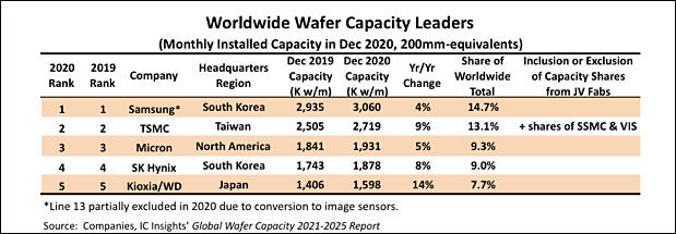
At present, according to analysts at Dalton Investments, three quarters of the world's production of complex semiconductor components is concentrated at TSMC and Samsung Electronics.
Moreover, if we consider 7nm and finer technical processes, then these companies control the entire volume of production. Intel's attempts to master 7nm technology have not yet materialized in the production of serial products
New duopoly is forming.
-
On March 4, 2021, as part of its ongoing efforts to realign its investments to focus on growth drivers and key markets and streamline its operations, ON Semiconductor Corporation (the “Company”) plans to implement certain employee terminations during the first half of 2021 (the “Employment Separations”). The Employment Separations will impact approximately 740 of the Company’s and its subsidiaries’ employees globally. The Company estimates that it will incur between $58 million and $62 million in aggregate costs during the first half of 2021.
The Company plans to reinvest a substantial portion of the savings generated from the Employment Separations into its continuing workforce and certain business initiatives and opportunities. Consequently, the restructuring may not result in a material reduction in the Company’s future operating expenses. The Company intends to continue to evaluate measures to realign its investments to achieve the Company’s strategic and transformational goals.
https://www.sec.gov/ix?doc=/Archives/edgar/data/1097864/000119312521069468/d131412d8k.htm
-
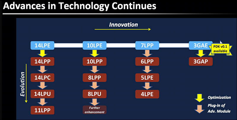
Samsung 3nm update
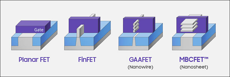
Samsung Foundry will be the first maker of semiconductors to start using gate-all-around field-effect transistor (GAAFET)-like structures with its upcoming 3 nm fabrication process. The node is not quite ready for primetime yet, but at the IEEE International Solid-State Circuits Conference (ISSCC) engineers from Samsung Foundry shared some of the details about the upcoming 3 nm GAE MBCFET (multi-bridge channel FET) manufacturing technology.
Formally, there are two types of GAAFETs: typical GAAFETs called nanowires that feature 'thin' fins as well as MBCFETs called nanosheets that use 'thicker' fins. In both cases, the gate material surrounds the channel region on all sides. Actual implementations of both nanowires and nanosheets heavily depend on design, so in general many industry observers describe both with one term, GAAFETs. But previously they were known as surrounding-gate transistors (SGTs). Meanwhile, MBCFET is a trademark of Samsung.
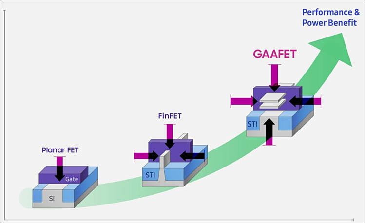
The first GAAFETs were demonstrated in 1988, so the key advantages of the technology are pretty well known. The very structure of this type of transistor allows designers to precisely tune them for high performance or low power by adjusting width of the transistor channel (also known as effective width, or Weff); wider sheets enable higher performance at higher power while thinner/narrower sheets reduce power consumption and performance. To do something similar with FinFETs, engineers have to use additional fins in a bid to improve performance. But in this case the 'width' of the transistor channel can only be doubled or tripled, which is not really precise and sometimes inefficient. In addition, adjustments of GAAFETs allow for increased transistor density, as different transistors can be used for different purposes.

 sa16702.jpg749 x 458 - 34K
 sa16703.jpg800 x 269 - 28K
 sa16704.jpg800 x 407 - 50K
 -
TSMC, United Microelectronics (UMC), Vanguard International Semiconductor (VIS) and Powerchip Semiconductor Manufacturing (PSMC) continue to run at full capacity for their 28nm and above process technologies.
Most factories are able to drop 28nm and above prices by 2-3 times if they will add new production lines, but they are not doing it for years (say thanks to cartel agreements). Because they want simple way to get big money.
Howdy, Stranger!
It looks like you're new here. If you want to get involved, click one of these buttons!
Categories
- Topics List23,964
- Blog5,723
- General and News1,342
- Hacks and Patches1,151
- ↳ Top Settings33
- ↳ Beginners254
- ↳ Archives402
- ↳ Hacks News and Development56
- Cameras2,361
- ↳ Panasonic990
- ↳ Canon118
- ↳ Sony154
- ↳ Nikon96
- ↳ Pentax and Samsung70
- ↳ Olympus and Fujifilm99
- ↳ Compacts and Camcorders299
- ↳ Smartphones for video97
- ↳ Pro Video Cameras191
- ↳ BlackMagic and other raw cameras121
- Skill1,961
- ↳ Business and distribution66
- ↳ Preparation, scripts and legal38
- ↳ Art149
- ↳ Import, Convert, Exporting291
- ↳ Editors191
- ↳ Effects and stunts115
- ↳ Color grading197
- ↳ Sound and Music280
- ↳ Lighting96
- ↳ Software and storage tips267
- Gear5,414
- ↳ Filters, Adapters, Matte boxes344
- ↳ Lenses1,579
- ↳ Follow focus and gears93
- ↳ Sound498
- ↳ Lighting gear314
- ↳ Camera movement230
- ↳ Gimbals and copters302
- ↳ Rigs and related stuff272
- ↳ Power solutions83
- ↳ Monitors and viewfinders339
- ↳ Tripods and fluid heads139
- ↳ Storage286
- ↳ Computers and studio gear560
- ↳ VR and 3D248
- Showcase1,859
- Marketplace2,834
- Offtopic1,319


