
-
Panasonic says it has developed an image sensor 100 times as sensitive to light as existing technology, enabling self-driving cars to spot pedestrians, traffic signals and other objects instantly even at night.
The Japanese manufacturer aims to have a practical version ready as early as 2020 or so.
With the race to build road-ready autonomous cars heating up, so too is the competition in the electronics needed to make them work.
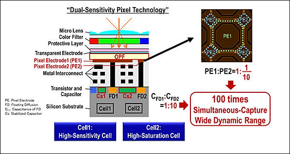
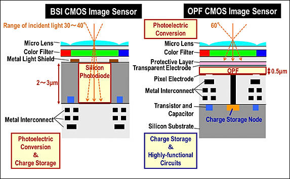
The company's new design is made from a thin film of organic material rather than silicon, the stuff of most microchips. Panasonic developed the basic technology with Fujifilm. A proprietary circuit design reduces noise when converting light to electrical signals, while a modified electrode structure helps detect even faint light efficiently.
Conventional image sensors tend to get blinded by headlights or other sources of glare -- a shortcoming that limits their ability to discern objects at night. Panasonic says its new sensor is sharp-eyed enough to make out the license plate number of a speeding car. The company envisions a range of uses besides self-driving cars, including surveillance cameras and medical equipment.
Of course with real current QE sensor can not be even 2 times more efficient, it is just marketing speak made for stupid journalists.
-
More normal PR
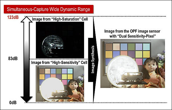
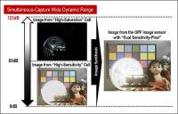
Panasonic Corporation today announced that it has developed a new wide-dynamic-range[1] technology which can improve simultaneous-capture wide dynamic range[2] 100 times wider than the conventional results, using a CMOS image sensor with an organic photoconductive film (OPF)*2.
In OPF CMOS image sensor, charge-storage function and photoelectric-conversion function can be set independently. By utilizing this unique feature of the OPF CMOS image sensor, overexposure can be prevented in bright situations without time distortion against moving object. And a sharp and texture-rich image can be reproduced even in dark situations. These technologies enable high-speed, high-precision imaging without time distortion in high-contrast scenes.
http://news.panasonic.com/press/news/data/2016/02/en160203-5/en160203-5.html
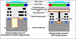
Panasonic Corporation today announced that it has developed a new highly functional global shutter[1] technology for CMOS image sensor using organic photoconductive film (OPF)1. This technology enables to capture high speed moving object up to 10 times brighter2 scene in global shutter mode. In OPF CMOS image sensor, charge-storage function and photoelectric-conversion function can be set independently. By utilizing the unique feature of OPF CMOS image sensor, this technology solves the degradation of saturation signal[2] in conventional image sensor with global shutter function. Motion direction can be detected from acquired object's signal level in one picture by fine control of shutter sensitivity by changing applied voltage to OPF which is hardly realized by conventional CMOS image sensors.
http://news.panasonic.com/press/news/data/2016/02/en160203-6/en160203-6.html
-
Useful images

 zebra863.jpg597 x 317 - 46K
 zebra864.jpg585 x 375 - 45K
 zebra865.jpg573 x 354 - 50K
 zebra866.jpg597 x 305 - 40K
 -
Well, we probably won't see a "sensitivity miracle" as touted, but maybe this sensor design will at least inspire future camera sensors with global shutter, something really still too rare/expensive.
-
Some pros opinion
Kazuko Nishimura presented the paper on the large HDR sensor with a low noise level. A few remarks about this sensor :
- HDR is obtained by two light sensitive areas within one pixel : one with low and one with high sensitivity. This is a very similar method as proposed long time ago by Fuji in their SuperCCD,
- The pixels do suffer from kTC noise, but by means of a cleaver circuit/feedback, they are able to reduce the remaining kTC noise to 1.2 e- reset noise and to 5.4 e- overall. In combination with a full well of 600 ke-, it creates a gorgeous dynamic range,
- The process used to fabricate the sensor is 65 nm CMOS, 1P3Cu1Al,
- The results mentioned are overall not bad, but there was no information provided about dark current, about quantum efficiency, about uniformity and about reliability of the material. So this suggests (to me) that there are still some issues to solve.
Sanshiro Shishido presented the paper on the global shutter version of the organic photoconductor sensor. The top plate of the photoconductor is made out of ITO and needs to be biased to larger voltages. But the overall light sensitivity of the organic photoconductor depends strongly on the exact voltage on the ITO gate. A lower voltage on the ITO gate lowers the light sensitivity and actually 0 V on the gate makes the sensor even blind. In this way one can create a global shutter functionality to the sensor. Moreover, one has the possibility to modulate the sensitivity during the exposure time, for instance, the exposure time can be split in parts in which the sensor will be sensitive and in parts in which the sensor will be insensitive. Even one has the option to modulate the sensitivity during the periods the sensor is sensitive by means of adapting the high voltage set to the ITO gate. Overall a nice technology !
Howdy, Stranger!
It looks like you're new here. If you want to get involved, click one of these buttons!
Categories
- Topics List23,972
- Blog5,724
- General and News1,348
- Hacks and Patches1,153
- ↳ Top Settings33
- ↳ Beginners255
- ↳ Archives402
- ↳ Hacks News and Development56
- Cameras2,360
- ↳ Panasonic990
- ↳ Canon118
- ↳ Sony155
- ↳ Nikon96
- ↳ Pentax and Samsung70
- ↳ Olympus and Fujifilm100
- ↳ Compacts and Camcorders299
- ↳ Smartphones for video97
- ↳ Pro Video Cameras191
- ↳ BlackMagic and other raw cameras118
- Skill1,961
- ↳ Business and distribution66
- ↳ Preparation, scripts and legal38
- ↳ Art149
- ↳ Import, Convert, Exporting291
- ↳ Editors191
- ↳ Effects and stunts115
- ↳ Color grading197
- ↳ Sound and Music280
- ↳ Lighting96
- ↳ Software and storage tips267
- Gear5,414
- ↳ Filters, Adapters, Matte boxes344
- ↳ Lenses1,579
- ↳ Follow focus and gears93
- ↳ Sound498
- ↳ Lighting gear314
- ↳ Camera movement230
- ↳ Gimbals and copters302
- ↳ Rigs and related stuff272
- ↳ Power solutions83
- ↳ Monitors and viewfinders339
- ↳ Tripods and fluid heads139
- ↳ Storage286
- ↳ Computers and studio gear560
- ↳ VR and 3D248
- Showcase1,859
- Marketplace2,834
- Offtopic1,319


