It allows to keep PV going, with more focus towards AI, but keeping be one of the few truly independent places.
-
Intel 10nm pushed to 2022 at least (most probably it is total toast)
Leaked roadmaps from Dell people.
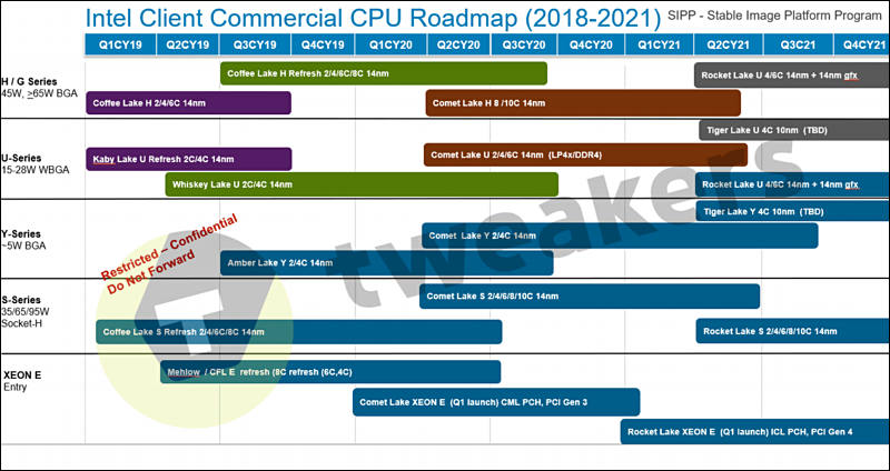
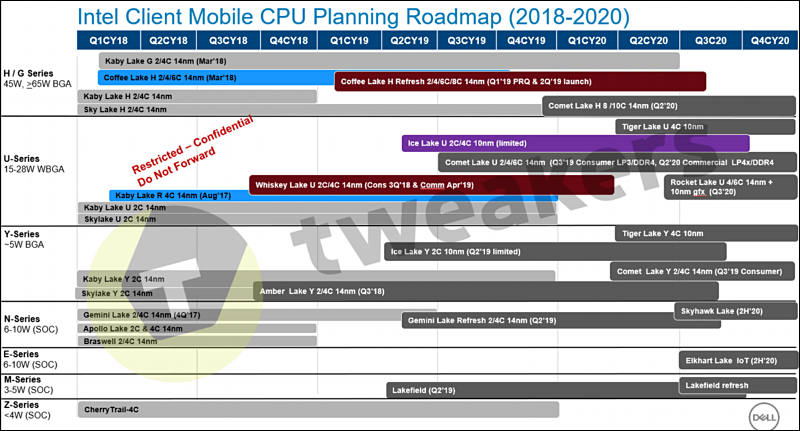
Next year Intel plans to add another 2 cores while keeping same deficient double channel memory system, and this time thermal throttling will be real severe.

 sa8061.jpg800 x 424 - 78K
 sa8062.jpg800 x 431 - 81K
 -
Not only 10nm is not ready, it will be slower even in Intel dreams
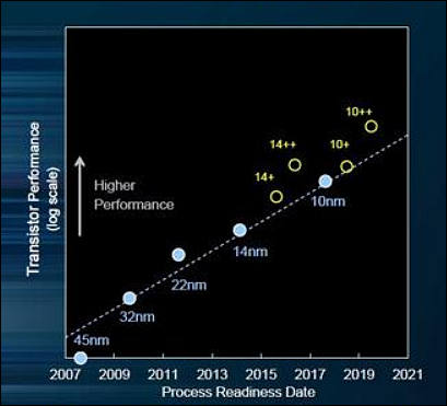
AMD approach with chiplets is much smarter, but be ready to expect lot of bad surprises in Zen 2.

 sa8064.jpg409 x 371 - 21K
 -
AMD goals
- AMD publically assured that they believe that TSMC could keep up with demand, this means that issue is present and actual
- AMD plans to increase CPU prices
- AMD hence plans to increase gross margin to 41% this year and up to 44% next year as they try to move as much money into investors pockets as possible
- We will see repeat of smartphones and cameras market issues in next 2 years in CPU market.
-
Recent reports indicate that the 7nm node is expensive, thus leading several large players to scale back product development on leading nodes, thus leaving about 10 percent of TSMC’s 7nm production capacity underutilized.
Strange reports.
-
New Intel PR
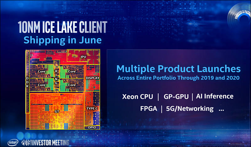
10nm Process Technology: Intel’s first volume 10nm processor, a mobile PC platform code-named “Ice Lake,” will begin shipping in June. The Ice Lake platform will take full advantage of 10nm along with architecture innovations. It is expected to deliver approximately 3 times faster wireless speeds, 2 times faster video transcode speeds, 2 times faster graphics performance, and 2.5 to 3 times faster artificial intelligence (AI) performance over previous generation products1. As announced, Ice Lake-based devices from Intel OEM partners will be on shelves for the 2019 holiday season. Intel also plans to launch multiple 10nm products across the portfolio through 2019 and 2020, including additional CPUs for client and server, the Intel® Agilex™ family of FPGAs, the Intel® Nervana™ NNP-I (AI inference processor), a general-purpose GPU and the “Snow Ridge” 5G-ready network system-on-chip (SOC).
The company plans to effectively deliver performance and scaling at the beginning of a node, plus another performance improvement within the node through multiple intra-node optimizations within the technology generation.
7nm Status: Renduchintala provided first updates on Intel’s 7nm process technology that will deliver 2 times scaling and is expected to provide approximately 20 percent increase in performance per watt with a 4 times reduction in design rule complexity. It will mark the company’s first commercial use of extreme ultraviolet (EUV) lithography, a technology that will help drive scaling for multiple node generations.
The lead 7nm product is expected to be an Intel Xe architecture-based, general-purpose GPU for data center AI and high-performance computing. It will embody a heterogeneous approach to product construction using advanced packaging technology. On the heels of Intel’s first discrete GPU coming in 2020, the 7nm general purpose GPU is expected to launch in 2021.
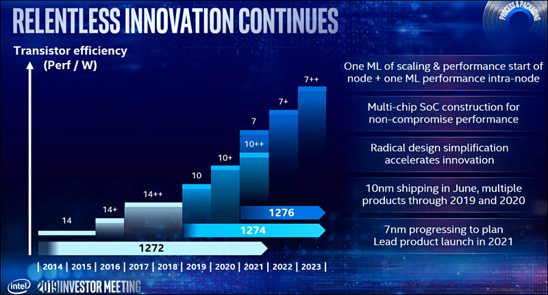

 sa8215.jpg800 x 467 - 89K
 sa8214.jpg800 x 431 - 74K
 -
Notes from SemiAccurate's CC about Intel
- Cannon Lake 10 nm, "launched" in 2017 with a single Lenovo China laptop, had single digit yields
- Charlie reported a "level of fear he had never seen" around then from Intel sources [Similar to Olympus]
- The original plan was for four fabs to move to 10 nm. 3 out of the 4, including one in each of Israel, Arizona, and Oregon, will NOT move to 10 nm.
- No info on what the 4th fab is doing, but at least 75% of the original 10 nm fab capacity is no longer there.
- COAG (Contact Over Active Gate) was to have saved INTC 10% in area. It completely failed, impacting integrated graphics. This is why the Q4 2017 10 nm Canon Lake had no iGPU
- 10nm is slower, and its yields are < 50% that of 14 nm.
- The recently leaked Dell roadmaps confirm that the INTC 2017 claim that 10 nm and 10nm+ processes will be behind on performance compared to 14 nm.
- Ice Lake 10 nm will only be the low performance end of the stack. It will also come in 14 nm variants.
- High core count and performance as well as AI with Bfloat 16 will remain at 14 nm.
- All INTC custom foundry customers have bailed, including Cisco, Panasonic, and LG. The entire INTC custom foundry effort was a flaming disaster.
- Questioned about INTC 14 nm shortages, Charlie mentions (previously behind the paywall) that this was driven by massive hits to server customers from Spectre and Meltdown security flaws, which drove volume buys to restore capacity [China buys ahead of tariffs in Intel speak].
So, this diversion played well.
- AMD Rome delivers a 1.6x performance delta over INTC's current and for the next year Cascade Lake.
- AMD will have a 50 to 60% server CPU performance advantage until at least late 2021.
- AMD Milan will have an amazing 15 chiplets.
- AMD is pushing chiplets very hard.
-
TSMC plans considering 5nm (marketing ones)
TSMC has already kicked off risk production of 5nm chips, said the report, adding that the process is expected to be ready for commercial production in the second quarter of 2020 when the phase-one facility of the foundry's new Fab 18 comes online.
Dubbed N5+, namely 5nm Plus, the process node will feature both performance and power consumption advances, according to a recent Chinese-language Commercial Times report. The foundry is expected to move N5+ to risk production in the first quarter of 2020, the report said.
-
Sales of smartphones in the China market tumbled by 31.3% on quarter and 16.7% on year to 71.7 million units in the first quarter of 2019.
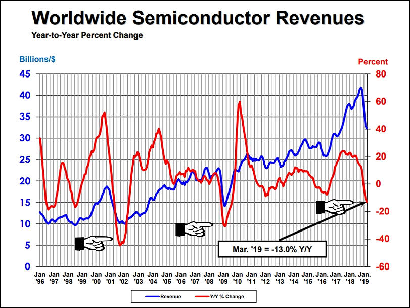
Big dangers for semiconductors progress ahead, as with development costs rising exponentially drop on smartphone market can lead to disaster.
-
Intel started to think about separating factories
While during recent meeting they told that no such plans this year exist, but they also told that they will return to such option within 2020. If we will see 10nm/7nm still not working we can see extremely fast and sudden merger or separation. So, such we can be already to only 2 companies competing in 2021 (Samsung and TSMC).
-
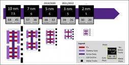
TSMC now hopes to scare competition with 2nm plans
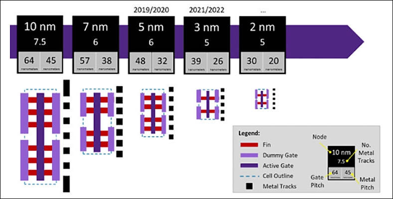
One of their top managers told that they plan to make new factory tailored for 2nm processes soon, near their upcoming 5nm plant.
Unofficially they plan to have first commercial 2nm chips ready in 2024.
I highly doubt it, as one of them main reasons of TSMC winning this round had been misleading marketing calling real 10-11nm process as 7nm.
So, most probably nice graphics on top will be in reality significantly different and we can see some new marketing stunts.
Global foundries, of course, also never had 12nm process that AMD used for previous Ryzen chips, it had been just renamed and improved 14nm, ala Intel 14nm+++.
 sa8755.jpg789 x 399 - 47K
 -
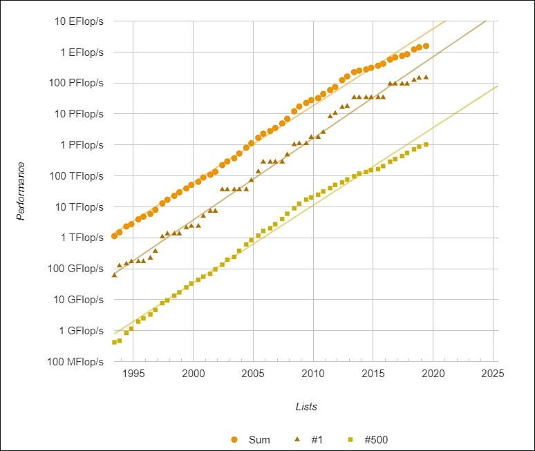
How slowing down progress look at supercomputers chart

 sa8790.jpg774 x 653 - 58K
 -
Samsung can start making 14nm chips, including CPUs for Intel
Intel stopped any further investment in failed 10nm process.
Korean Sedaily leaked that from Q4 of 2019 Samsung will start making 14nm products for Intel. Most probably it'll be only first deal part, as Intel for now do not have any working advanced processes, with 10nm lines being able to make only 10nm 2 core chips with huge failure rates (up to 95%).
7m, and further 5nm processes could be necessary for Intel to survive, and such way we will be down to only two companies who will continue to making any progress in semiconductors manufacturing.
-
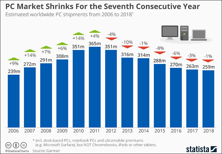
Same as 2011 had been year of 2500K, 2019 is the year of Ryzen 3xxx, and will be next peak before even faster reduction. Industry won't be able to scale further from 16 cores without drastic price increases and thermal output increase.
-
“It's going to keep going,” said Jim Keller, a semiconductor rock star who joined Intel last year as senior vice president of silicon engineering, and a cohost of the event. “Moore’s law is relentless”
“The working title for this talk was ‘Moore’s law is not dead but if you think so you’re stupid,’" he said Sunday. He asserted that Intel can keep it going and supply tech companies ever more computing power. His argument rests in part on redefining Moore’s law. “I’m not pedantic about Moore’s law talking just about transistors shrinking—I’m interested in the technology trends and the physics and metaphysics around that,” Keller says. “Moore’s law is a collective delusion shared by millions of people.”
Keller said Sunday that Intel can sustain that delusion, but that smaller transistors will be just one part of how. On the conventional side, he highlighted Intel’s work on extreme ultraviolet lithography, which can etch smaller features into chips, and smaller transistor designs based on nano-scale wires due to arrive in the 2020s.
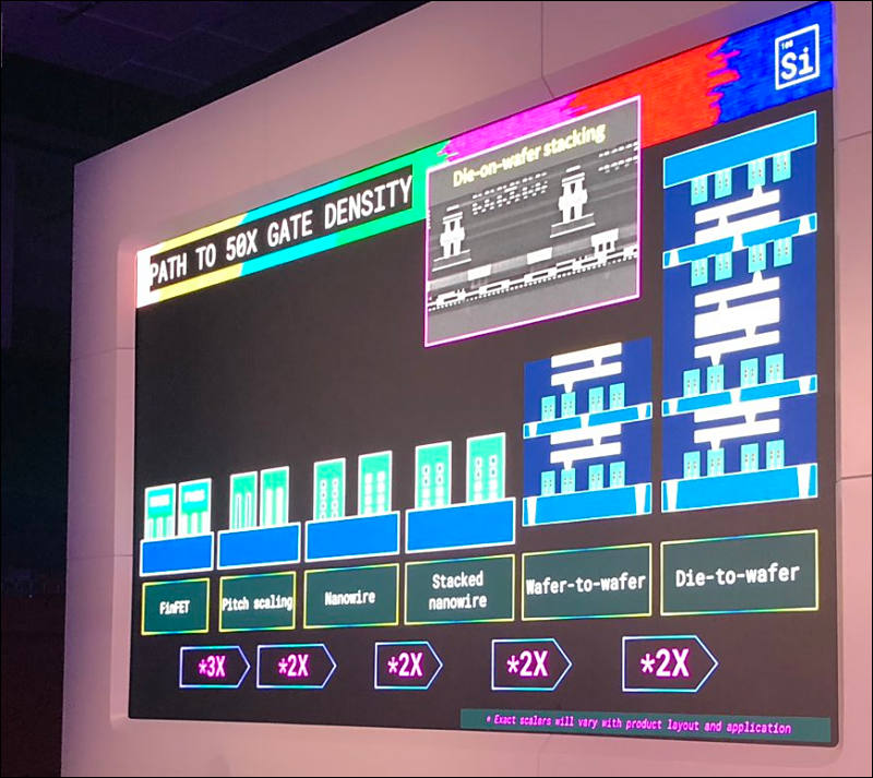
Keller also said that Intel would need to try other tactics, such as building vertically, layering transistors or chips on top of each other. He claimed this approach will keep power consumption down by shortening the distance between different parts of a chip. Keller said that using nanowires and stacking his team had mapped a path to packing transistors 50 times more densely than possible with Intel's 10 nanometer generation of technology. “That’s basically already working,” he said.
All this vertical 3D stuff does not work for heavy load chips like CPUs. Only for their SRAM and IO parts may be.
-
Some chips cost estimation table
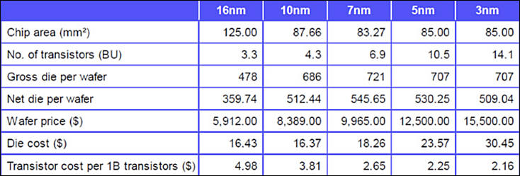
Btw, TSMC 7nm yields for not too large chips like AMD Zen 2 reached 80-85% now.
For previous process on same stage it had been around 90-95%.
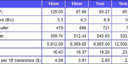
 sa9102.jpg734 x 249 - 53K
 -
Interesting slides
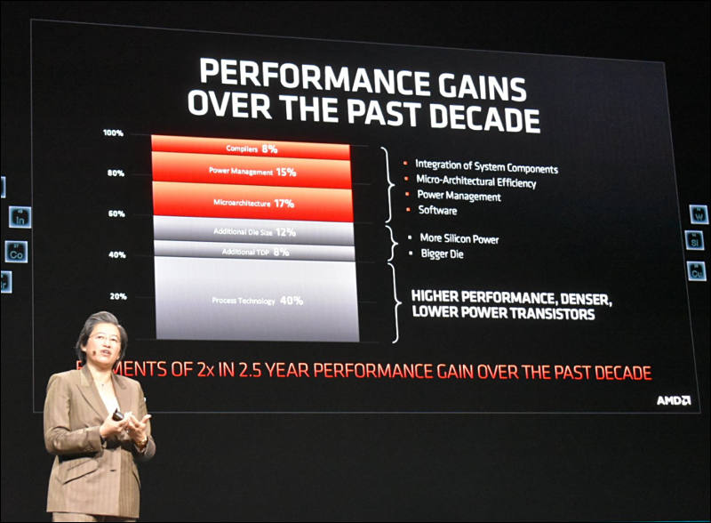
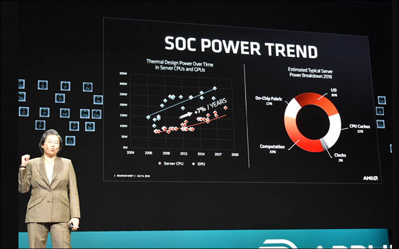
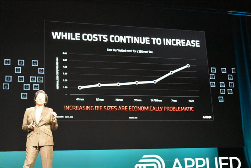
-
How it looks in smartphone space
With rising heat dissipation demand from major vendors including Samsung Electronics, LG Electronics, Huawei, Oppo and Xiaomi for their 5G smartphones, half of cooling module shipments for smartphones in the second half of 2019 will be vapor chamber-based solutions, and the other half heatpipe-based ones, according to industry sources.
And it is only small beginning.
Fall of smartphone huge market will be unprecedented and it will destroy some of leading semiconductors manufacturers.
-
Watch how capitalism criminals work
Wafer processing equipment sales will fall 19.1% in 2019 to US$42.2 billion. The other front-end segment, consisting of fab facilities equipment, wafer manufacturing, and mask/reticle equipment, is expected to slide 4.2% to US$2.6 billion this year. The assembly and packaging equipment segment is on track to decline 22.6% to US$3.1 billion in 2019, while semiconductor test equipment is forecast to decrease 16.4% to US$4.7 billion this year.
Most of this issues are due to DRAM and NAND manufacturers trying to return to huge 300-600% margins by cutting output.
-
3nm marketing nanometers will be tough
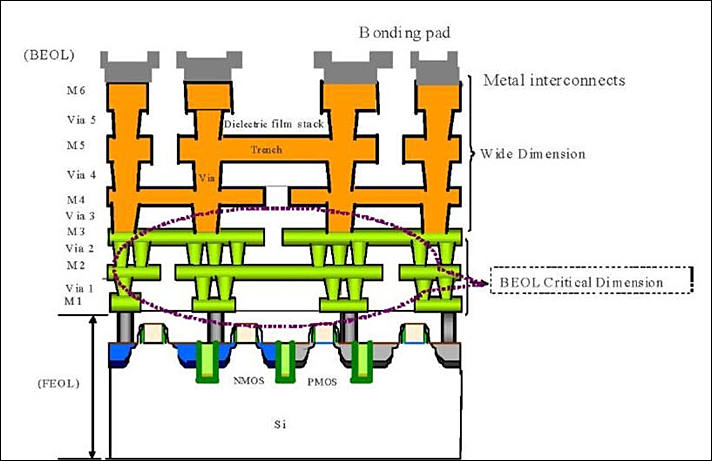
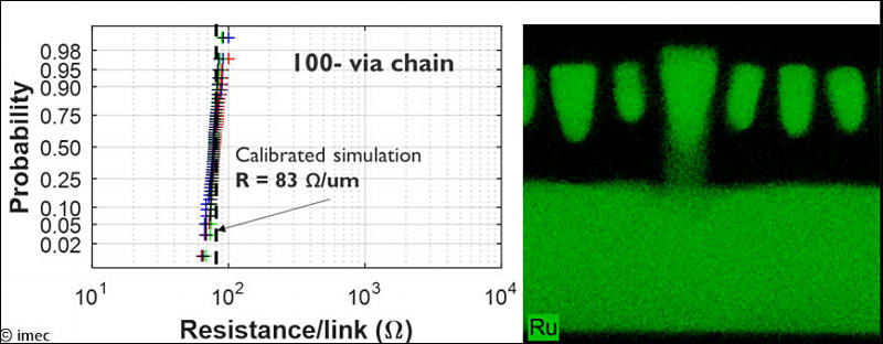
This week, at its technology forum ITF USA 2019, imec, a world-leading research and innovation hub in nanoelectronics and digital technologies, presents a dual-damascene 21nm pitch test vehicle relevant for manufacturing the 3nm logic technology node. With this test vehicle, a 30 percent improvement in resistance-capacitance product (RC) was obtained compared to previous generations, without impacting reliability. The need for implementing scaling boosters such as self-aligned vias and self-aligned blocks in 3nm and beyond interconnect technologies has been demonstrated.
-
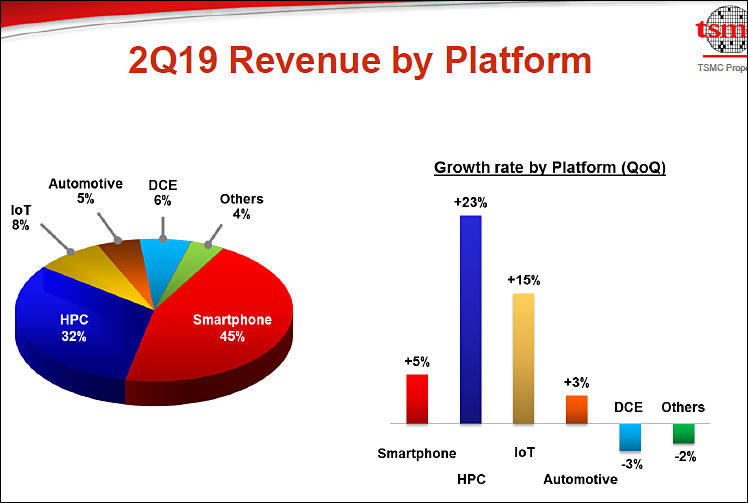
AMD processors play more significant role in TSMC revenues
-
Moore’s Law has run out of gas, “and that is profound,” said Victor Peng, CEO of Xilinx.
“You can get one of the three, it’s hard to get two of three, and I would challenge anyone who says they can get three of the three,” he said. Today’s extreme ultraviolet (EUV) lithography systems only remove the complexity of multi-patterning today’s chips, the 7-5-3-nm names of the latest nodes “are all marketing numbers, and no one has fixed the interconnect problem.”
“The cost of designing a 5-nm chip will be astronomical,” limiting the node’s use to a few companies who “can amortize it across multiple designs. Because of the constraints of Moore’s Law, you have to work harder — there’s no freebie in optical scaling anymore.”
Howdy, Stranger!
It looks like you're new here. If you want to get involved, click one of these buttons!
Categories
- Topics List23,964
- Blog5,723
- General and News1,342
- Hacks and Patches1,151
- ↳ Top Settings33
- ↳ Beginners254
- ↳ Archives402
- ↳ Hacks News and Development56
- Cameras2,361
- ↳ Panasonic990
- ↳ Canon118
- ↳ Sony154
- ↳ Nikon96
- ↳ Pentax and Samsung70
- ↳ Olympus and Fujifilm99
- ↳ Compacts and Camcorders299
- ↳ Smartphones for video97
- ↳ Pro Video Cameras191
- ↳ BlackMagic and other raw cameras121
- Skill1,961
- ↳ Business and distribution66
- ↳ Preparation, scripts and legal38
- ↳ Art149
- ↳ Import, Convert, Exporting291
- ↳ Editors191
- ↳ Effects and stunts115
- ↳ Color grading197
- ↳ Sound and Music280
- ↳ Lighting96
- ↳ Software and storage tips267
- Gear5,414
- ↳ Filters, Adapters, Matte boxes344
- ↳ Lenses1,579
- ↳ Follow focus and gears93
- ↳ Sound498
- ↳ Lighting gear314
- ↳ Camera movement230
- ↳ Gimbals and copters302
- ↳ Rigs and related stuff272
- ↳ Power solutions83
- ↳ Monitors and viewfinders339
- ↳ Tripods and fluid heads139
- ↳ Storage286
- ↳ Computers and studio gear560
- ↳ VR and 3D248
- Showcase1,859
- Marketplace2,834
- Offtopic1,319


